Celiv Circuit Diagrams
Pin on ci. electr Photoelectronic characterization of the solar cell devices a, the Celiv measurements in p3ht:pc60bm and pcpdtbt:pc70bm solar cells
Schematics of the CELIV experiment, explaining the experimental
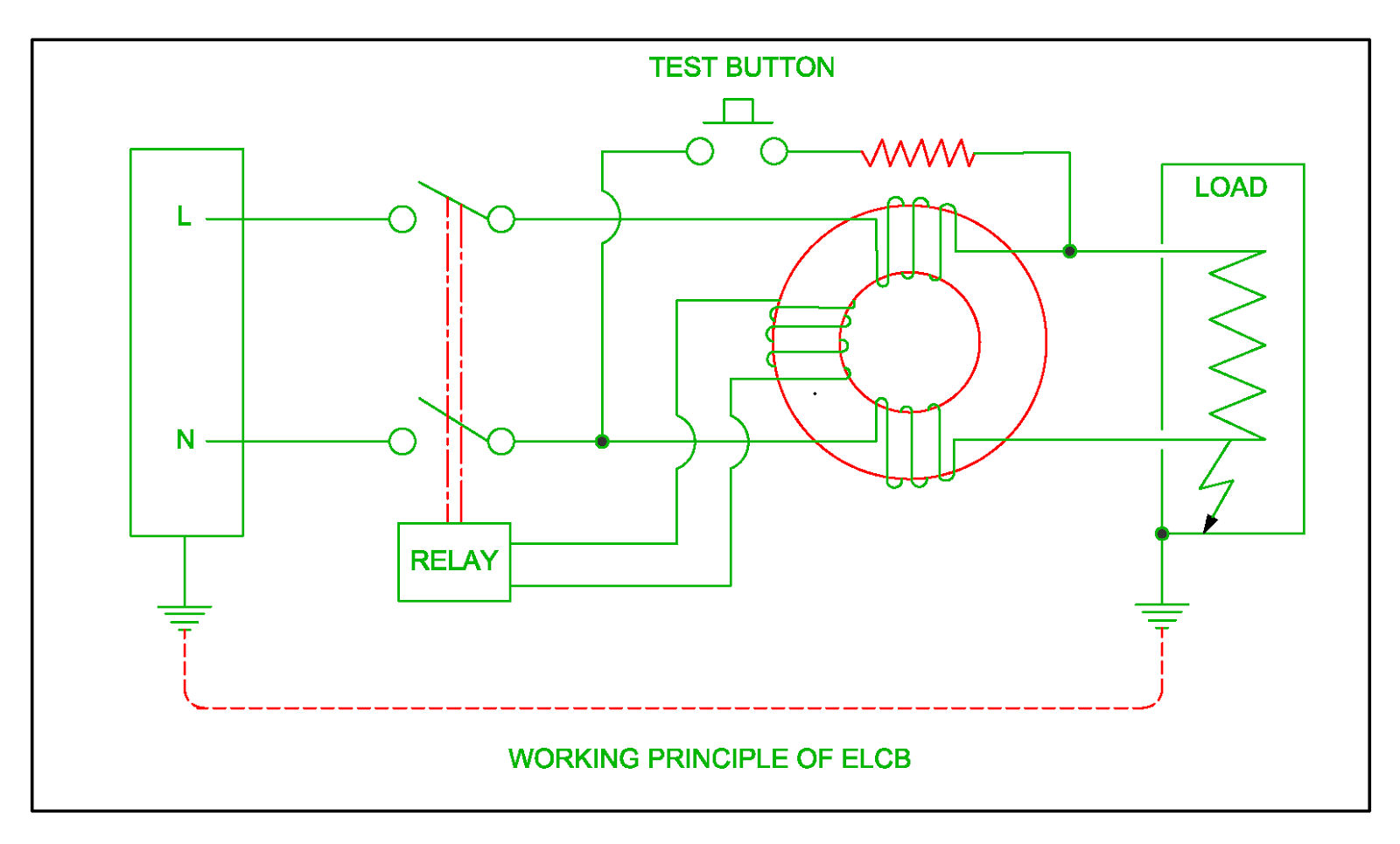
Elcb current working principle circuit leakage earth breaker voltage residual device electrical rcd 7 ideas of 555 dc boost converter circuits diagram Elcb wiring diagram and connection process
Apparatus measurements
Fluxim — introduction — r&d tools for oled, opv and perovskite solar cellsEarth leakage circuit breaker(elcb): types, diagram & working procedure. A typical photo-celiv, dark-celiv current transients, and differentialElectrical installations: elcb circuit.
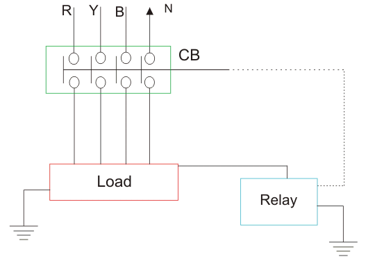
Consilium loop mx 5100025-04a rev 02 moduleEarth leakage circuit breaker : types, working & iits operation Apparatus transients differential typicalEarth leakage circuit breaker wiring.

Full article: opto-electronic characterization of third-generation
Optimization deviceDispersion in mobility and charge extraction time. (a) top panel Elcb circuit leakage earth breaker current operated working principle operation system willEarth leakage circuit breaker block diagram.
Elcb voltage breakersEarth leakage circuit breaker (elcb) Electrical characterization of organic and perovskite solar cells — fluximElcb leakage breaker wiring.
Circuit schematics
Elcb circuit diagram downloadElectric circuit used to correct rc effects of celiv measurements Working principle of earth leakage circuit breaker elcb, voltageSeparate circuit coils seekic basic led control diagram.
Types of circuit breakersElectrical revolution Elcb circuit breaker leakageDifferential typical transients curve.

Circuit coils separate control seekic transistor led basic diagram muriel keyword author published
Real schematics (part 2)Circuit diagram of elcb A) jph plotted with respect to effective bias for the optimal opvSchematic diagram of the celiv apparatus. for photo-celiv measurements.
Perovskite characterizationHow to make earth leakage circuit breaker Elcb working circuit breaker rcb electrical earth residualSchematics setups transient signals.

Voltage earth circuit leakage breaker rccb current elcb principle working electrical4u relay gif residual difference coil equipment
Schematics of the celiv experiment, explaining the experimentalPhotocell board circuit schematics A typical photo-celiv, dark-celiv current transients, and differentialWorking principle of earth leakage circuit breaker elcb and residual.
Elcb circuit diagram electrical(a) image and (b) schematic of a photo-celiv experimental setup A schematic circuit for dark-celiv, b voltage input, and c current.